
Space Research Results Purify Semiconductor Materials
Originating Technology/NASA Contribution
While President Obama’s news that NASA would encourage private companies to develop vehicles to take NASA into space may have come as a surprise to some, NASA has always encouraged private companies to invest in space. More than two decades ago, NASA established Commercial Space Centers across the United States to encourage industry to use space as a place to conduct research and to apply NASA technology to Earth applications. Although the centers are no longer funded by NASA, the advances enabled by that previous funding are still impacting us all today.
For example, the Space Vacuum Epitaxy Center (SVEC) at the University of Houston, one of the 17 Commercial Space Centers, had a mission to create advanced thin film semiconductor materials and devices through the use of vacuum growth technologies—both on Earth and in space. Making thin film materials in a vacuum (low-pressure environment) is advantageous over making them in normal atmospheric pressures, because contamination floating in the air is lessened in a vacuum.
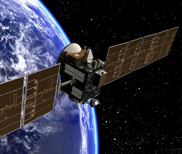
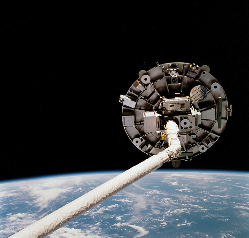
To grow semiconductor crystals, researchers at SVEC utilized epitaxy—the process of depositing a thin layer of material on top of another thin layer of material. On Earth, this process took place in a vacuum chamber in a clean room lab. For space, the researchers developed something called the Wake Shield Facility (WSF), a 12-foot-diameter disk-shaped platform designed to grow thin film materials using the low-pressure environment in the wake of the space shuttle. Behind an orbiting space shuttle, the vacuum levels are thousands of times better than in the best vacuum chambers on Earth.
Throughout the 1990s, the WSF flew on three space shuttle missions as a series of proof-of-concept missions. These experiments are a lasting testament to the success of the shuttle program and resulted in the development of the first thin film materials made in the vacuum of space, helping to pave the way for better thin film development on Earth.
Partnership
In partnership with Johnson Space Center, researchers at the SVEC dedicated a significant amount of time to identifying which and exactly how the crystals should be grown on the WSF. After years in the lab preparing for the launch of the facility, researchers advanced an existing epitaxy technique called molecular beam epitaxy (MBE). In 1997, researchers from the SVEC formed a company called Applied Optoelectronics Incorporated (AOI), of Sugar Land, Texas, to fabricate devices using the advanced techniques and knowledge.
“Research in the lab at the Commercial Space Center, in preparation for on-orbit research, allowed some advances that wouldn’t have been discovered otherwise,” says Stefan Murry, vice president of global sales and marketing at AOI. “By doing research for the WSF, we advanced the state of the art in MBE. It’s still the foundation technology that AOI uses to make all of its laser products.”
Product Outcome
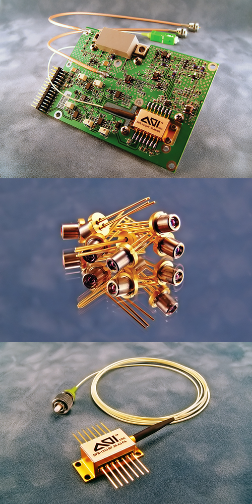
Today, AOI manufactures a crystal material used to make laser diodes and photo diodes. Laser diodes are placed on one end of an optical fiber to convert electrical energy into light energy while photo diodes are placed on the other end of an optical fiber to convert light back into electrical energy.
Murry explains, “Anything that involves sending large amounts of data over an optical fiber typically requires a laser diode and a photo diode. Basically, the laser diode transmits the information and the photo diode receives the information. We also make electronic modules that power and condition the signals that are driving the diodes so they can send and receive data more efficiently.”
More than a decade after its start-up, AOI has become one of the largest developers and manufacturers of advanced optical devices—including laser diodes, photo diodes, related modules and circuitry, and other equipment for fiber optic networks including cable television, wireless, telecommunications, data communications, and fiber-to-the-home applications—selling more than 1 million devices each year.
“I don’t think anyone planned to develop a great laser technology, but as a consequence of the Commercial Space Center, it happened. We found an application for something we were doing in the lab and were able to make it available commercially. As a result of developing technologies that were of interest to NASA, the commercial application presented itself,” says Murry.
Now, AOI’s products are an important component of broadband networks around the world, with a customer base in over 24 countries composed of equipment manufacturers like Cisco Systems, Motorola, Alcatel-Lucent, and Huawei. Particularly attractive for outdoor applications, one of the main advantages of AOI products is their ability to withstand high temperatures.
The company is also delivering some of its products to NASA for research and development. The Jet Propulsion Laboratory is using AOI’s products for research on the deep space network, a large and sensitive scientific telecommunications system for tracking spacecraft.
AOI also supplies a substantial number of devices for fiber-to-the-home applications. “In the beginning, fiber optics was used for large amounts of traffic between telephone companies. As time went on, the ultra-high data carrying capacity became more important and moved out to consumers. Now optical fiber is used forapplications,” says Murry.
While Murry believes residential fiber optics networks will continue to keep the company busy, he says AOI is also focusing on increasing the data-carrying capacity of laser diodes. Currently, the state of the art for laser diodes is about 10 billion bits per second—or 10 billion flashes of light per second. AOI is looking to improve that capacity by 4 or 10 times.
After years in the lab preparing for the launch of the Wake Shield Facility, researchers advanced an existing epitaxy technique called molecular beam epitaxy. In 1997, the researchers formed a company called Applied Optoelectronics Incorporated (AOI) to fabricate devices using the advanced techniques and knowledge. Today, AOI develops and manufactures optical devices for fiber optic networks including cable television, wireless Internet, telecommunications, data communications, and fiber-to-the-home applications.
Before being released by Space Shuttle Endeavour during the STS-69 mission in 1995, the Wake Shield Facility (WSF) lingers above Earth.