

Semiconductor Cubing
A Memory Short Stack (Memory Short Stack is a trademark of Irvine Sensors Corporation.) is a three-dimensional semiconductor package in which dozens of integrated circuits are stacked one atop another to form a cube. Known as "chip-stacking" or "cubing," the innovative process was invented by Irvine Sensors Corporation (ISC), Costa Mesa, California from technology developed under NASA and Department of Defense contracts. The cubing technique offers faster processing speeds, higher levels of integration and lower power requirements than conventional chip sets; it also offers dramatic reduction in the size and weight of memory-intensive systems such as medical imaging devices.
ISC's cubing technology is regarded as a major advancement in high density computer electronics. The Memory Short Stack won a 1993 NASA Award of Innovation and in 1994 was selected by R&D Magazine for an R&D 100 Award, presented annually to the year's 100 most technologically significant new products.
ISC initiated its stacking technology development in the early 1990s. Department of Defense contracts led to development of a "full stack" version of the technology, but the height of the full stack was too great for the multichip packages employed in airborne and spaceborne electronic systems, the primary market envisioned at that time. The company therefore embarked on development of the Memory Short Stack concept, which involved a more limited number of chips mounted like a stack of pancakes. This approach lowered the height of the stack, permitted its attachment using conventional surface-mounting techniques, and broadened the number of electronics packages in which it could be used.
The Memory Short Stack that evolved from the company's development effort is fabricated by vertical assembly of integrated circuits, thinned to as little as seven-thousandths of an inch, and extremely thin layers of laminate. This configuration significantly increases density and maximizes efficient use of design space. Typically, cubes average between 40 and 50 integrated circuits.
Although ISC originally focused on military and space applications of 3D chip-stacking, it is now introducing the technology to a broadening range of commercial market applications, including computers and telecommunications. The company has established a joint development program with IBM Corporation, Burlington, Vermont and is exploring other alliances with major computer manufacturers. Current ISC products include a four-megabit Wide Word Memory Short Stack and DRAM Memory Short Stacks in 64-, 80- and 160-megabit configurations.
Under the Small Business Innovation Research (SBIR) program, NASA has awarded Irvine Sensors eight Phase I and five Phase II contracts, including an ongoing project at Jet Propulsion Laboratory (JPL) to evaluate chip-stacking for space systems. The NASA contracts contributed importantly to the commercialization of the cubing technology. One of them, sponsored by Goddard Space Flight Center, involved application of the Memory Short Stack to a spaceborne data recorder. That project significantly advanced the commercialization potential because it called for designing the short stacks so that they would be compatible with such industry standard attachment techniques as wire-bonding and tape-automated bonding; this configuration made Memory Short Stacks usable in virtually all types of electronic assemblies.
In addition, the Goddard SBIR attracted the attention of IBM Corporation and led to the ISC/IBM partnership designed to facilitate high volume, cost-competitive production of short stacks for the commercial market. ISC and IBM share a Cubing Process Development Center at Essex Junction, Vermont. Deliveries of the first Memory Short Stacks produced at Essex Junction began in 1994.
Another NASA contract of special importance is a JPL contract for a processing node known as SOBIEC (Spacecraft On Board Information Extraction Computer). This work takes the 3D stacking technology one step further by combining Memory Short Stacks with parallel processing. The commercial potential for this advancement of the technology is described as "enormous."
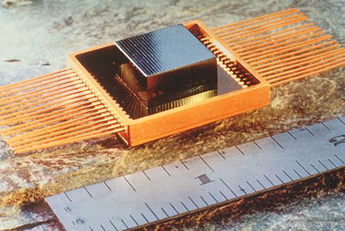
A Memory Short Stack is a cube-shaped package of integrated circuits.
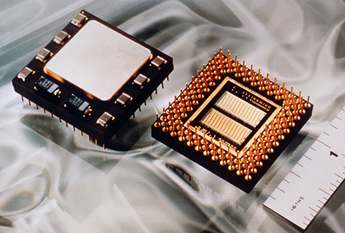
An advanced development for a NASA spacecraft computer combines 3D stacking with parallel processing.
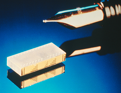
The DRAM 80-Megabit Short Stack exemplifies the small size of the stacked package.


