
Cleaning up Silicon
Ultra-high purity silicon is ideal for the production of computer chips. For this reason, a space-based manufacturing technique, developed in the 1970s, has found a coveted place in the semiconductor industry. Thanks to the help of NASA's Jet Propulsion Laboratory (JPL), Advanced Silicon Materials, LLC--formerly Advanced Silicon Materials, Inc. (ASiMI)is producing silane gas and ultra-high purity polycrystalline silicon (polysilicon) at very high volume.
In 1975, Union Carbide Corporation, entered a development program with JPL for a low-cost, high-volume silane process as part of the Low Cost Silicon Solar Array Project. From that original contract, Union Carbide was able to harness a manufacturing process that went from producing small amounts of silane to one that could yield silane in commercially viable quantities. Later on, Union Carbide's research was expanded to develop a process that would convert metallurgical-grade silicon to silane gas and ultra-high purity polysilicon.
Union Carbide built a small pilot plant that manufactured silane to supply the production of ultra-high purity polysilicon for electronic devices. By 1985, a full-scale commercial plant for producing silane and polycrystalline silicon was built in Moses Lake, Washington. In 1990, ASiMI acquired the rights to the Union Carbide technology and built a second production facility in 1998 in Butte, Montana.
ASiMI's high-volume manufacturing operation produces silane and ultra-high purity silicon through a four-step distillation process, which begins with the gasification of metallurgical-grade silicon--a compound that contains impurities, such as iron, aluminum, and manganese. Gasifying the impure silicon involves grinding it down to a fine, sand-like consistency and super-heating it with hydrogen and silicon tetrachloride. Through a series of reactions and separation steps, silane and ultra-high purity polysilicon are produced.
Silane was previously manufactured in small batch facilities and distributed in individual gas cylinders. Only applications that could make use of minor quantities of silane were practiced. With the operation of Union Carbide's original pilot plant, the technology for bulk shipment of silane was also developed. The advantages of having a substantial amount of a consistently high-quality source material appealed to semiconductor manufacturers.
The availability of bulk quantities of silane fostered the commercial development of new applications outside of the traditional electronics industry. Today, silane is finding new uses in the manufacturing processes of energy efficient glass coatings, thin film transistors, photosensitive copier drums, and photovoltaics. In the semiconductor industry, silane is used for several process steps, such as epitaxial, polysilicon, nitride, oxide, and silicide films. The ultra-high purity of silane is a key factor in its use in these demanding applications.
The purity of silane is 99.9999 percent. Electronically active impurities, such as boron, phosphorus, and arsenic are controlled to less than 10 parts per trillion, making silane one of the purest materials on Earth.
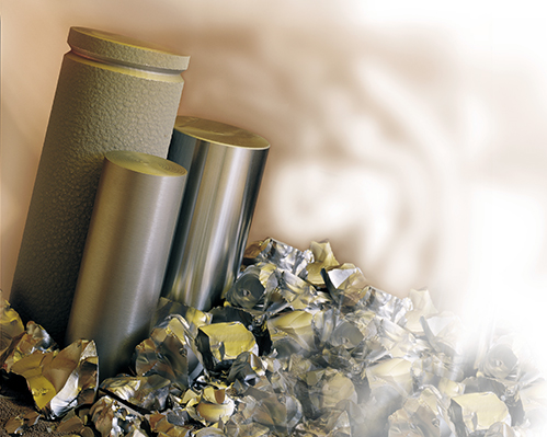
ASiMI's high-volume manufacturing operation produces bulk quantities of silane.