Novel Nanotube Manufacturing Streamlines Production
Originating Technology/NASA Contribution
Nanotubes are sheets of graphite, one atom thick, rolled into seamless cylinders, with an exterior diameter in the range of nanometers. For a sense of perspective, if you were to split a human hair into 50,000 independent strands, a nanotube would be about the size of one of those strands.
What would someone do with anything that small? These nanostructures have novel qualities that make them uniquely qualified for a plethora of uses, including applications in electronics, optics, and other scientific and industrial fields.
These thin, hollow tubes have remarkable strength, especially considering their microscopic size. Stronger than steel, nanotube strands can be used to form extremely strong, yet lightweight, materials. They are efficient conductors of heat (able to withstand temperatures up to 2,000 °C in the absence of oxygen) and also possess unique electrical properties. Nanotubes can be manufactured so that they conduct electricity as well as copper, but can also be made to function as semiconductors (able to switch from conducting electricity to insulating from it), making them quite valuable in the production of miniaturized electronic components.
Although scientists have been aware of these nanostructures since their discovery in 1991 by Japanese physicist Dr. Sumio Iijima, practical use has been thwarted by the high costs, complexity, and even danger of manufacturing them. A group of researchers at Goddard Space Flight Center, led by Dr. Jeannette B. Benavides, however, developed a manufacturing process for single-walled carbon nanotubes (SWCNTs) that overcomes these obstacles.
Typical methods for creating these nanostructures, whether chemical vapor deposition, laser ablation, microwave, or high-pressure carbon monoxide conversion, use metal catalysts to encourage the carbon to grow into the tube shape, as opposed to capping and sealing. The NASA process uses helium arc welding to vaporize an amorphous carbon rod and then form nanotubes by depositing the vapor onto a water-cooled carbon cathode, which then yields bundles, or ropes, of single-walled nanotubes at a rate of 2 grams per hour using a single setup.
The NASA-developed process eliminates the costs associated with the use of metal catalysts, including the cost of product purification, resulting in a relatively inexpensive, high-quality, very pure end product. The process employs an arc welder, a helium purge, an ice water bath, and basic processing experience. This significantly simplifies previous complex, dangerous manufacturing processes, which required expensive equipment like vacuum chambers, dangerous gasses, and extensive technical knowledge.
While managing to be less expensive, safer, and simpler, the process also increases the quality of the nanotubes. Since no metal catalyst is used, no metal particles need to be removed from the product. The elimination of these metal impurities increases the temperature at which the materials will degrade and eliminates any damage that may have been caused by purification processes used to remove metal residue.
Partnership
In 2003, Benavides filed a New Technology Report at Goddard, bringing her invention to the attention of the Center’s Innovative Partnerships Program (IPP) office, which acknowledged the role this production process could play in making carbon nanotubes more accessible. The IPP office started the process of finding commercial partners.
To get this cutting-edge process into the hands of the public, Goddard’s IPP office promoted the technology in print, online, and at industry conferences. In 2005, the technology captured the interest of Wayne Whitt, an entrepreneur interested in forming an advanced materials corporation, but who was in search of an innovation that would help his company stand out from the crowd. Shortly after learning about the SWCNT manufacturing technology, Whitt applied for a nonexclusive license and formed the Boise-based Idaho Space Materials Inc. (ISM).
Product Outcome
Once the license was granted, ISM then worked with Benavides and the University of Idaho’s Electron Microscopy Center to examine and improve upon variables in the manufacturing process, ultimately enhancing the process by increasing yield and production capacity. Once the process was tweaked, ISM was ready to commercialize its products, and the inexpensive, robust nanotubes are now in the hands of the scientists who will create the next generation of composite polymers, metals, and ceramics that will impact the way we live. In fact, researchers are examining ways for these newfound materials to be used in the manufacture of transistors and fuel cells, large screen televisions, ultra-sensitive sensors, high-resolution atomic force microscopy probes, supercapacitors, transparent conducting films, drug carriers, catalysts, and advanced composite materials, to name just a few.
In August 2006, ISM unveiled its new line of single-walled nanotubes with no metal catalyst under the name NOMEC 1556. The advanced materials company has had tremendous success with its new product, and has nearly tripled in size.
The transfer of this NASA technology has also been beneficial to NASA, as widespread use of the Space Agency’s patented technology will produce revenue that NASA can reinvest in additional research, and it now has a reliable source from which to obtain high-quality, low-cost SWCNTs for use in its research and missions.
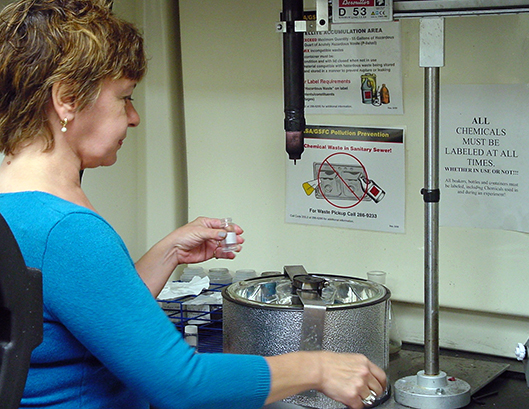
Unlike most current methods—which require expensive equipment (e.g., vacuum chamber), dangerous gasses, and extensive technical knowledge to operate—NASA’s simple SWCNT manufacturing process needs only an arc welder, a helium purge, an ice water bath, and basic processing experience.

NASA’s single-walled carbon nanotube (SWCNT) manufacturing process eliminates the costs associated with the use of metal catalysts, including the cost of product purification. As a result, the manufacturing cost can be reduced significantly for high-quality, very pure SWCNTs.


