
Low-Cost Sensors Deliver Nanometer-Accurate Measurements
NASA Technology
Carlos Capiro gathers his thoughts to relate how a single NASA sensor led to a product poised to disrupt his industry. “Really, a lot of it had to do with luck,” he begins.
Capiro, CEO of Juntura Group, was part of a team of MBA students at Rollins College near Orlando that in 2012 participated in the school’s Entrepreneurial Scholar of Distinction Program by lending their insight to NASA. Kennedy Space Center’s Technology Transfer Office had approached a professor at the school with a handful of patents it wanted better market analysis on. The professor in turn involved his students and had them evaluate the market potential of a NASA-patented technology—in this case, a sensor originally created to help scientists inspect space shuttle windows for damage caused by micrometeoroids.
Micrometeoroid impacts happen often in low-Earth orbit: at that height is a very thin cloud of naturally-occurring debris that whips around the planet at a rate of about six miles per second. And while most of it is smaller than a grain of sand, at those speeds even particles of dust can act like microscopic bullets on a surface, leaving behind craters and scratches that run fractions of an inch deep.
“The orbiter windows are fairly large,” says Dr. Robert Youngquist, who runs the Applied Physics Lab at Kennedy and worked with the scientists who inspected the shuttle windows after each mission. “They’re one-inch-thick pieces of quartz. But if these craters are deep enough, there’s a chance that the windows will fracture during the next launch from the aerodynamic pressure and heating they undergo.”
For years, the best available method to measure defects discovered in the shuttle windows involved liquefying dental mold and pouring it over the scratch. When the material hardened, it was peeled off and examined using a microscope. “It was the only technique they had,” explains Youngquist. “It worked, but not as well as you would want.”
At NASA’s request, Youngquist devised an alternative method. Instead of measuring nicks and cracks directly, Youngquist used an optical technique that employs a small mirror to track the surface of the window. What that meant for Youngquist’s team, he says, was that “we had transferred the problem of trying to measure these pits over to the problem of measuring the position of a mirror—and that’s a lot easier to do.”
The final piece of the puzzle was finding a small, energy-efficient sensor to measure the mirror’s movement with accuracy down to the length of a micron, or one ten-thousandth of a centimeter. When their search turned up empty, Youngquist decided to create one himself.
The resulting sensor required minimal hardware—only a few inductors, or small coils of wire that generate a magnetic field when an electrical current runs through them. Two fixed inductors on either side of the mirror generate opposing magnetic fields; when the third inductor, which tracks with the mirror, moves closer to either field, it picks up that signal. Youngquist’s team could measure those minute changes in magnetic fields and convert them into highly accurate measurements of the pits and cracks in the shuttle’s quartz windows.
Technology Transfer
When Kennedy’s Technology Transfer Office reached out to the MBA program at Rollins, Youngquist’s sensor was among the many technologies offered for analysis. “We showed them patents that we were passively marketing, technologies that could have benefited from additional work before bringing them to market,” says Jeff Kohler, who is a manager in the center’s Technology Transfer Office.
Reviewing the portfolio, the team of students came across Youngquist’s sensor and, feeling like they had discovered something special, got to work. “We had the right players involved,” says Capiro. “We all come from engineering backgrounds, and a couple of us had experience in business and finance.” The team members invested their own money to create a viable prototype of a commercial version of the sensor, as well as a marketing campaign to go with it. The effort paid off when, at the end of the semester, they presented a comprehensive analysis of the sensor’s market potential to Kohler, Youngquist, and other representatives from Kennedy.
“We were more than impressed with their presentation,” says Kohler. “They presented their prototype test kit in sealed boxes with a logo on it, showed us their extensive market research, and also expressed an interest in starting a company and seeing if they could take the technology somewhere.”
Immediately after, Capiro and four others formed Juntura Group Inc., based in Winter Park, Florida, and obtained an exclusive license to sell the sensor.
Benefits
Since acquiring the license, Juntura has continued to advance the technology, increasing its capability from the original resolution of 400 nanometers down to 10 nanometers—approximately the thickness of a cell wall.
With a capability applicable in a multitude of fields, the company has set its sights first on what Capiro calls “low-hanging fruit”: 3D printers, laser holders and beam-steering mirrors, military technology, and robotics. “Imagine our sensor integrated into each component, whether that be a laser holder or the joints of a robot,” he says. “Now you can tell in real time, with just a signal, ‘Is my setup in line and ready to go? Is the joint returning exactly to where it was before, ensuring the repeatability of my robot’s motion?’ Those are markets we’re aggressively going after.”
One of Juntura’s primary advantages is the low cost of the core technology. Whereas sensors with similar capabilities currently on the market can cost about $2,000 per unit, Capiro says his company aims to sell its product for close to $500. Juntura even hopes to appeal to the growing “maker” community of tinkerers who like to assemble their own complex electronics and devices from low-cost parts. “By integrating our sensor with a 3D printer, you’re able to create commercial-grade products right in your home. The resolution is so good that you’d be hard pressed to determine whether it was created through an injection mold or a print job,” he says.
Juntura’s sensors have recently been purchased by a researcher at the Florida Institute of Technology who is using 3D printers to produce human tissue. Bioprinters currently cost upwards of $2 million, and the client hopes to reduce that price to something closer to $50,000—something Juntura’s competitive prices help enable.
“Imagine being able to take one of these printers to Haiti or a country in Africa and printing out skin grafts for burn victims,” says Capiro. “I think we’re going to be part of changing the world, and we have NASA to thank for support in that.”
That worldwide perspective is an ambitious vision for a technology originally inspired by the inadequacy of liquefied dental mold. Capiro takes obvious pleasure in the way the technology has blossomed—perhaps partly due to luck, as he says, but also clearly the result of the hard work Juntura put in to make it viable.
“We’re a bunch of college kids who were able to create a fully functional business out of a simple patent and our dreams and aspirations. It’s turning into a pretty cool story to tell,” he says.

Juntura’s sensors have become part of 3D printers that may soon be found in remote areas, providing on-site medical care—such as printed skin grafts—that was not possible before.
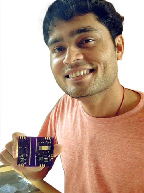
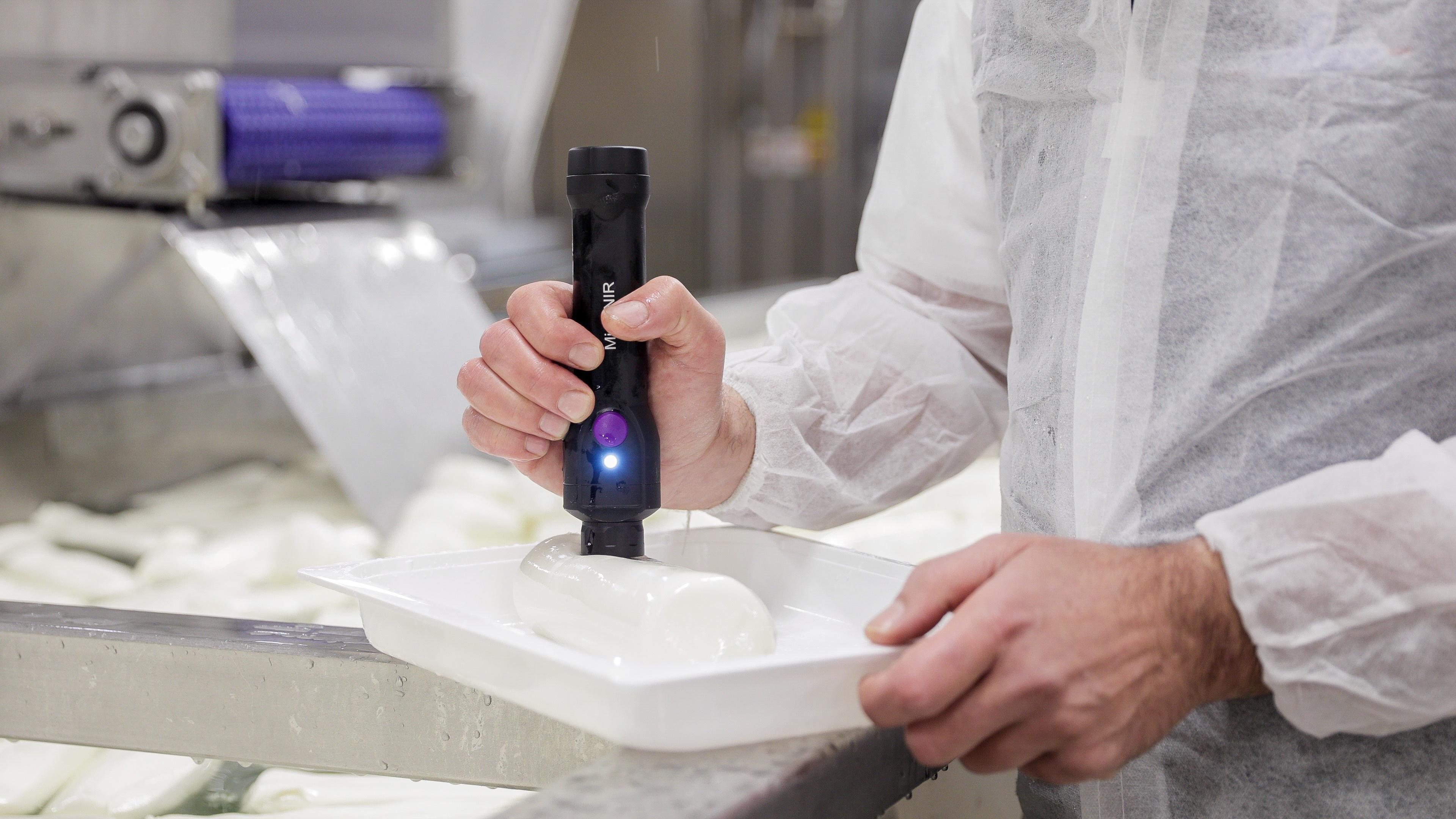
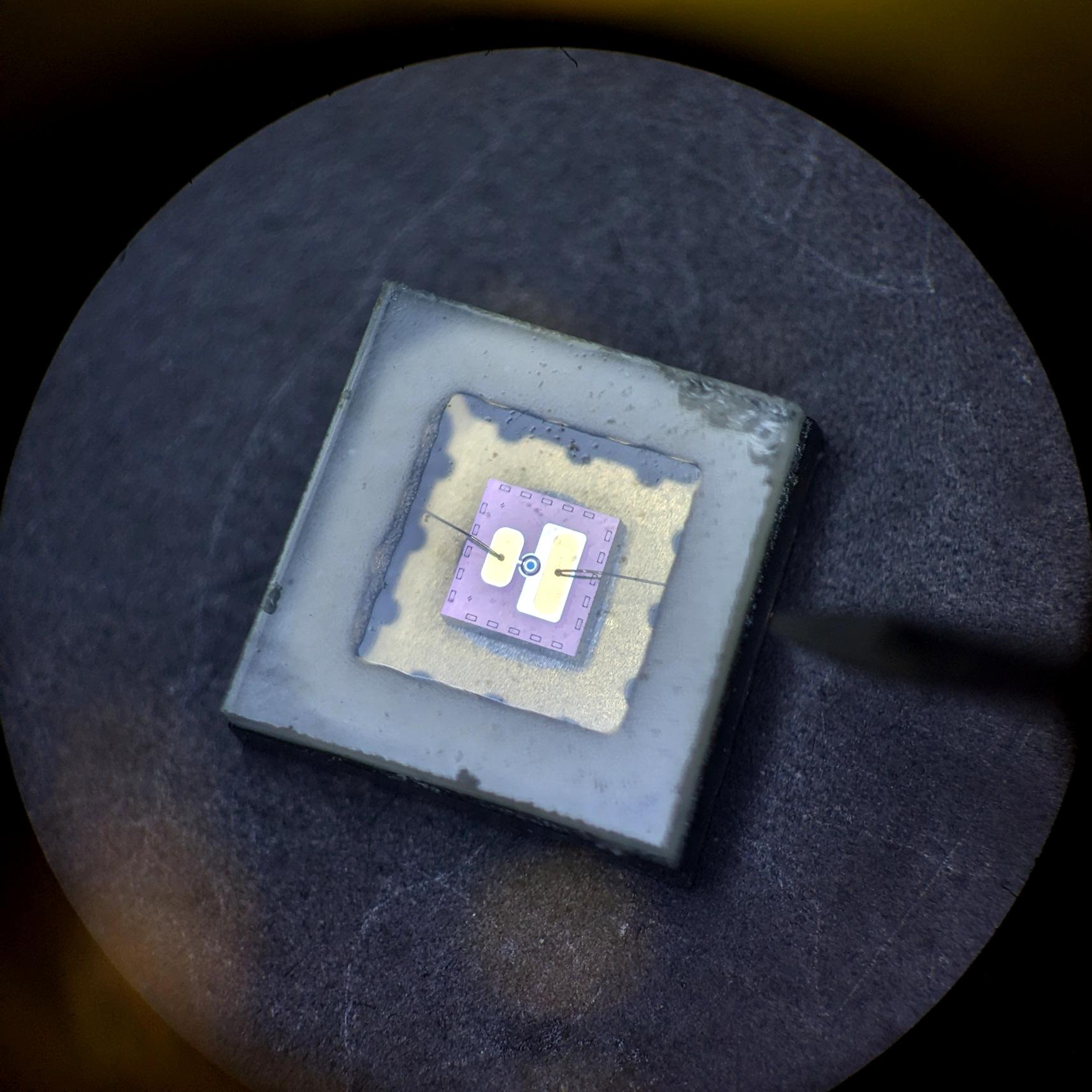
Juntura engineer Pankaj Patil holds a prototype of the company’s first position sensor.
The space shuttle’s windows were one-inch-thick pieces of quartz, but they required an inspection following each mission to locate microscopic scratches and cracks that could pose safety risks in subsequent launches.