Image Sensors Enhance Camera Technologies
Originating Technology/NASA Contribution
Buzz Aldrin standing on the stark surface of the Moon. The towering gas pillars of the Eagle Nebula. The rocky, rust-colored expanses of Mars. Among NASA’s successes in space exploration have been the indelible images the Agency’s efforts have returned to Earth. From the Hubble Space Telescope to the Hasselblad cameras in the hands of Apollo astronauts, many of NASA’s missions involve technologies that deliver unprecedented views of our universe, providing fuel for scientific inquiry and the imagination.
Less known than Hubble’s galactic vistas or the Mars rovers’ panoramic landscapes is the impact NASA has had on the era of digital photography on Earth. While the first digital camera was built by Eastman Kodak in 1975, the first to actually develop the concept of the digital camera was Jet Propulsion Laboratory (JPL) engineer Eugene Lally, who in the 1960s described the use of mosaic photosensors to digitize light signals and produce still images. During the following decades, NASA continued the work of developing small, light, and robust image sensors practical for use in the extreme environment of space.
In the 1990s, a JPL team led by Eric Fossum researched ways of improving complementary metal-oxide semiconductor (CMOS) image sensors in order to significantly miniaturize cameras on interplanetary spacecraft yet maintain scientific image quality. An image sensor contains an array of photodetectors called pixels that collect single particles of light, or photons. (The word “pixel”—short for picture element—was first published in 1965 by JPL engineer Frederic Billingsley.) The photons entering the pixel are converted to electrons, forming an electrical signal a processor then assembles into a picture. CMOS sensors represented a number of appealing qualities for NASA compared to the charge coupled device (CCD), the prevalent image sensor at the time. Crafted by the same process used to build microprocessors and other semiconductor devices, the CMOS image sensors can be manufactured more easily than CCDs and at lower cost. The CMOS sensor components are integrated onto a single chip, unlike CCDs, which have off-chip components. This integrated setup consumes as much as 100 times less power than CCDs, allows for smaller camera systems, and can be designed with radiation-hard pixel architectures for space applications.
At JPL, Fossum invented the CMOS active-pixel sensor (CMOS-APS), which integrates active amplifiers inside each pixel that boost the electrical output generated by the collected photons. The CMOS-APS featured improved image quality over passive-pixel sensors (without amplifiers) and included a number of on-chip functions, providing for complete miniature imaging systems that operate quickly with low power demands. JPL validated the technology through a series of prototypes.
Partnership
Fossum realized the CMOS-APS technology would be useful not only for imaging in space but on Earth as well. In 1995, he, his colleague and then-wife Sabrina Kemeny, and three other JPL engineers founded Photobit, based in Pasadena, California. Photobit exclusively licensed the CMOS-APS technology from JPL, becoming the first company to commercialize CMOS image sensors.
“We saw an expanding number of applications for these miniaturized cameras,” says Roger Panicacci, one of Photobit’s founders. The company quickly positioned itself on the cutting edge of the field of CMOS imaging, and by June 2000, it had shipped 1 million sensors for use in popular Web cameras, machine vision solutions, dental radiography, pill cameras, motion-capture, and automotive applications. The company was featured in Spinoff 1999 and founders Fossum, Panicacci, Kemeny, and Robert Nixon were inducted into the Space Foundation’s Space Technology Hall of Fame that same year.
In 2001, the company was acquired by semiconductor memory producer Micron Technology, of Boise, Idaho, and became a division of Micron Imaging Group. With the exploding popularity of the camera phone in the mid-2000s, the CMOS-APS proved ideal for crafting cameras that fit into slim cell phones and produce good photos without draining batteries. Riding the wave of camera phone demand, in 2006 the group became the world’s leading supplier of CMOS image sensors. In 2008, Micron Imaging Group was spunoff from Micron to form Aptina Imaging Corporation, based in San Jose, California. That same year, it shipped its 1 billionth sensor.
Product Outcome
Aptina has continued to improve on the original, NASA-developed CMOS-APS. The company has invented increasingly small pixel architectures, as well as a process for optimizing the amount of light that hits a pixel, boosting sensitivity and image quality while allowing the company’s customers to design more compact camera systems.
“Our technology is taking advantage of semiconductor innovation,” says Panicacci, now Aptina’s vice president of product development. “As transistors shrink, we can build smaller pixels, meaning that, in a given area of silicon, we can provide higher and higher resolution for products like camera phones.”
Aptina’s line of sensors allows for advanced camera features like electronic pan, tilt, and zoom, as well as applications requiring motion detection, target tracking, and image compression. The sensors are also incorporated into the company’s line of system-on-a-chip (SOC) devices—synergistic packages that enhance imaging, are easier and cheaper to integrate into products, and provide benefits like anti-shake compensation that corrects blurring from subject motion or an unsteady camera.
Aptina has grown from its NASA roots into a leader of the CMOS image sensor industry. Its sensors are currently integrated into one of every three cell phone cameras and are part of every major brand personal computer camera worldwide, as well as many embedded cameras for notebook computers. The company is also advancing CMOS sensors for digital still and video cameras—products that have traditionally featured CCD sensors, and has produced the first 10-megapixel CMOS image sensor for point-and-shoot cameras, a device that incorporates the company’s High Speed Serial Pixel Interface (HiSPi) capabilities, enabling a camera to create high-definition (HD) imagery.
The NASA-derived CMOS-APS can also be found in other, less obvious applications. Aptina produces tiny sensors for use in endoscopes for minimally invasive medical diagnostic procedures. The sensors do not generate potentially painful heat during examinations and are cheap enough to allow for disposable scope tubes, eliminating potential complications from improperly sterilized scopes. The company also worked with a medical imaging partner to develop the PillCam, an ingestible camera for imaging a patient’s gastrointestinal tract.
The automotive and surveillance industries represent other major markets for Aptina’s sensors. Major international auto brands like Daihatsu and Volvo employ Aptina designs for applications like backup cameras that help with parking and ensure safe reverse motion. Aptina estimates its customers will be building up to 25 million backup camera systems annually by 2011, potentially reducing backover accidents by about 20,000 per year. The company also has partnerships within the field of network surveillance, designing imaging technology that can spot cheating in casinos or intruders in unauthorized areas.
Last year, Aptina became a stand-alone company, and while Photobit once saw 1 million sensors shipped as a major milestone, says Panicacci, Aptina often ships over 1 million sensors a day. As demand rises for high-end capabilities like HD imaging and the market for camera products booms, Aptina’s NASA-developed technology should play an even greater role in products benefiting the public every day. Research by the International Data Corporation, an independent market research company, predicts annual sales of more than 1 billion camera phones beginning in 2010, all featuring one or more CMOS-APS cameras.
HiSPi™ is a trademark of Aptina Imaging Corporation.
PillCam® is a registered trademark of Given Imaging Ltd.
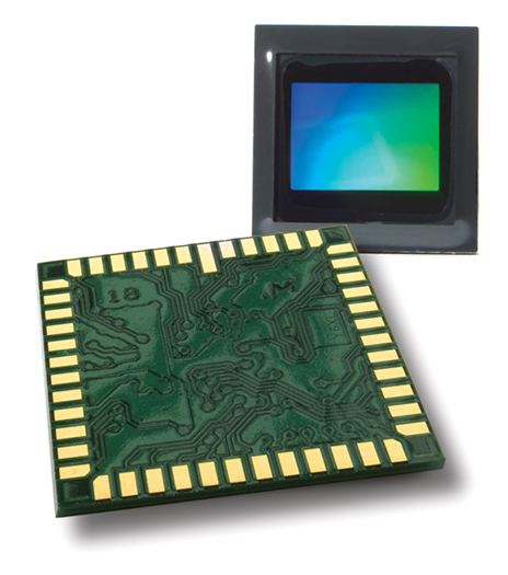
Aptina Imaging Corporation’s 10-megapixel complementary metal-oxide semiconductor sensor is the first such device for point-and-shoot cameras.



Images like these (from top) of the Eagle Nebula, Apollo 11 astronaut Buzz Aldrin on the Moon, and the Martian landscape bring the wonders of space exploration down to Earth.

Since the first human expeditions in space, astronauts have always carried cameras to capture the experience for everyone on the ground. Here an astronaut snaps a self-portrait during a spacewalk.


