
High Temperature Semiconductor Process
You may not be aware of their presence, but you are likely benefiting from them on a daily basis. Thin film processes are pervasive throughout government, industry, and the consumer world; used in computer read/write heads, semiconductor, and flat panel display manufacturing.
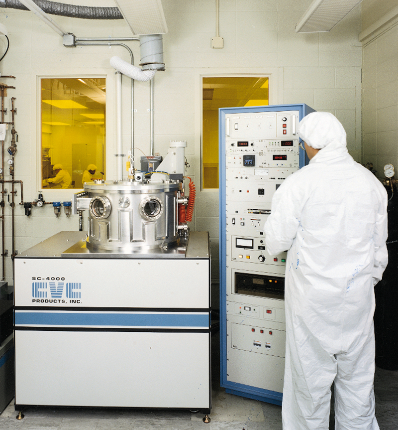
A sputter deposition system for depositing thin films was developed by CVC, Inc. of Rochester, New York, with the support of Jet Propulsion Laboratory's (JPL) Small Business Innovation Research (SBIR) program. The SC-4000 deposition system was developed for JPL to produce high quality films of high temperature superconducting material for microwave communication system components. The system was also used to deposit ferroelectric material for capacitors and the development of new electro-optical materials.
"This project placed CVC in a much better position within the industry and led to the turnaround of CVC's research and development efforts in thin film process solutions for a number of applications, such as aluminum oxide and copper, that have become commercially successful for CVC," comments Zoe Piliero, Director of Corporate Communications.
NASA applications for a thin film deposition system rested on production of high performance microwave system components, including power dividers, combiners, switched filters, and phase shifters utilizing superconducting material films.
CVC developed a unique sputter deposition system capable of depositing thin films of high temperature conducting material over relatively large areas.
Work on the deposition system set in motion sales of over $1 million, further strengthening the company's ability to provide deposition services. Assisted by the JPL SBIR support, CVC has become a leader in creating products and thin film process solutions.
The earlier SC-4000 sputter deposition system had five basic modules: the pumping system, baseplate, process chamber, control center, and load lock. A virtually unlimited combination of options and accessories was available for users of the deposition system. The system was equipped with high temperature heat, substrate rotation, thermal evaporation sources, ion gun, electron beam guns, and auto process controls. A range of oxides, selenides, and silicides was used for resistance, semiconductor, and photoconductive thin films.
For sputtering, the CVC hardware featured a microcomputer-based quartz crystal monitor that displayed thickness and deposition rates in real time. In an evaporation process mode, the quartz crystal monitor sensor was located within the evaporation area. One sensor was supplied with each evaporation source.
The sputter deposition system developed by CVC became an important tool for researchers who were developing ferroelectric capacitors and new electro-optical components for the communication systems of the future. In addition, the system enabled the use of high temperature superconducting materials in microwave communication systems, improving their efficiency and performance. High temperature superconductor films for microwave devices are ideal, as microwave losses are far below that of copper.
A worldwide supplier of thin film process equipment for semiconductor integrated circuits and thin film magnetic recording head manufacturing, CVC's annual revenues more than doubled in fiscal year 1996 over 1995, highlighted by the company's growth in the Asian markets, with 1997 also a banner year.
CVC's current thin film processing system, CONNEXION®, currently ranges in price from $1.5 million to $3 million, depending on the number of modules and features selected with the system configuration. CVC has an installed base of over 260 process modules on more than 80 CONNEXION cluster tool platforms.
Recording head, semiconductor, and flat panel display technologies continue to evolve day by day. CVC's goal is to continually invest in research and development and to improve equipment and process performance--placing them as a world leader by providing customers with the very best thin film process solutions.
®CONNEXION is a registered trademark of CVC, Incorporated.
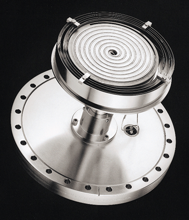
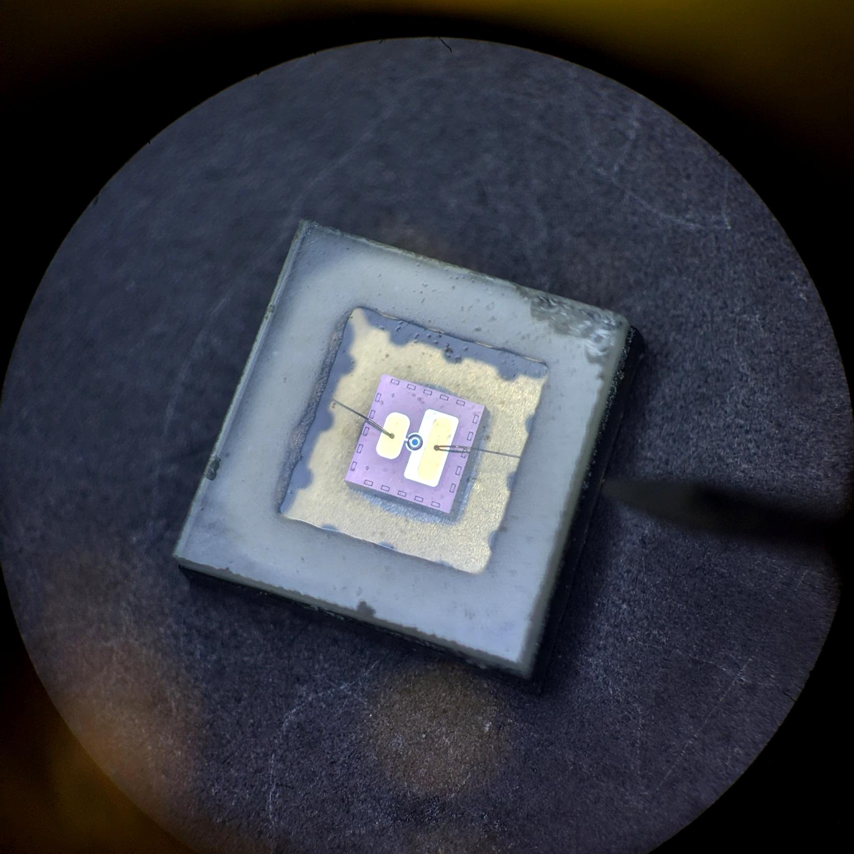
Substrate heating unit is made of inconel. High temperatures reached by the heater are key to depositing superconducting thin films.
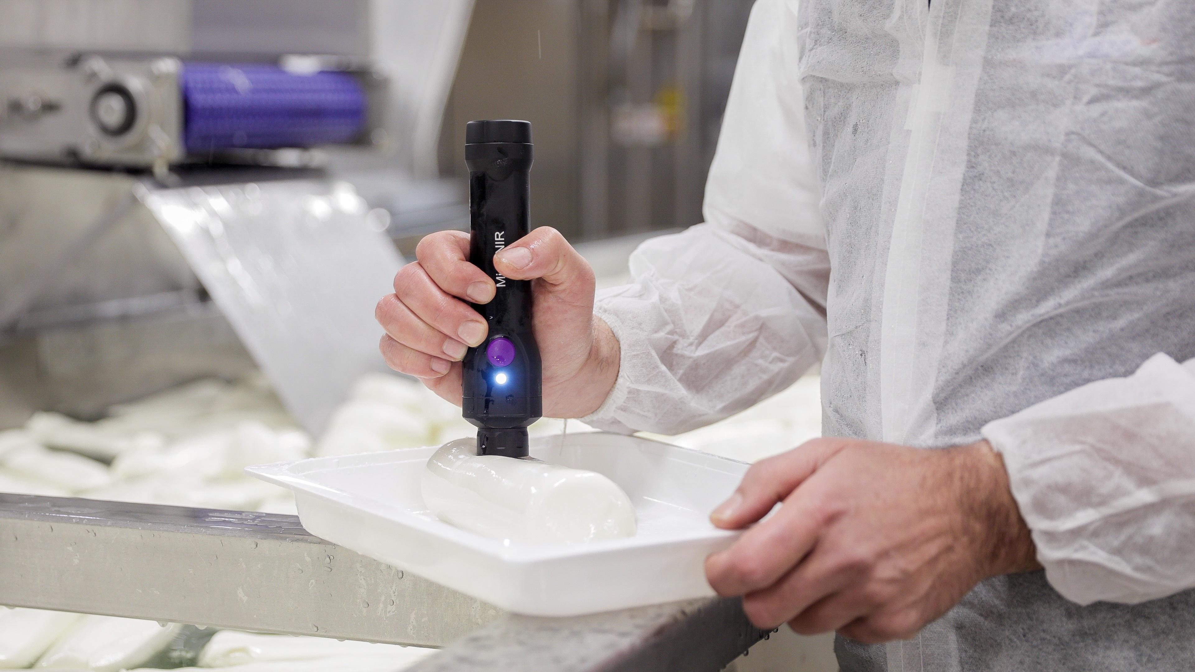
Specialist prepares CVC’s system for depositing superconducting thin films.