
Plasma Improves 3D Electronics Printing
Subheadline
Space Foundry’s plasma jet printer makes it easier to build electronics components on Earth and in space
A new approach to printing electronic components simplifies on-site manufacturing of electronics in space and on Earth.
With help from NASA funding and licensed technologies, San Jose, California-based Space Foundry has designed a plasma-based 3D printing process for electronics that has a number of advantages over other techniques. For one thing, it’s a single-step approach that doesn’t require heat or ultraviolet curing, as other methods do.
Eliminating the curing step, especially in space, “is huge logistically because you have to plan everything around astronaut up time,” said Ian Small, an electrical engineer at NASA’s Marshall Space Flight Center in Huntsville, Alabama.
Post-print curing can also be a challenge on Earth, where, in addition to the added infrastructure needed for curing, some of the printed materials oxidize quickly in the atmosphere. Copper, for example, which is useful in electronics because it’s highly conductive, is a challenge to cure and difficult to print on temperature-sensitive platforms.
Space Foundry has developed the hardware, software, and process for printing copper and other electronic materials without curing. The copper solution, as with any print material – or “ink” – introduced to the Space Foundry printing process, is aerosolized and then split apart by the plasma to create positive and negative ions, radicals, and electrons that react with the plasma. Print materials may undergo oxidation or reduction, depending on what electronic properties need adjusting for a particular material; the makeup of the plasma controls the adjustments.
“The uniqueness of their process, going through that plasma, lets them leverage some fancy chemistry,” said Small, who works on the NASA side of Space Foundry research backed by Small Business Innovation Research (SBIR) funding.
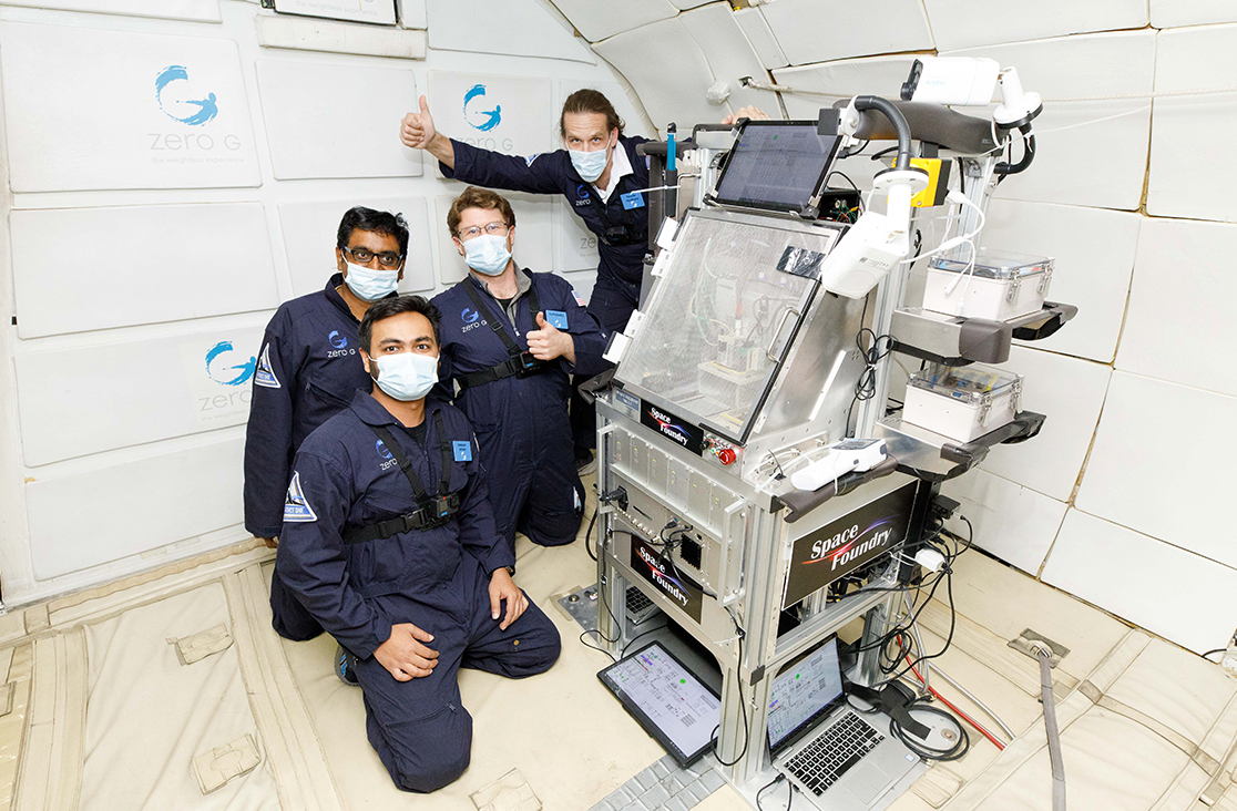
NASA’s Ames Research Center in Silicon Valley, California, has awarded the company four SBIR contracts to test its plasma jet printing technology, including in a microgravity environment, though much of the work is being overseen by Marshall.
Space Foundry cofounder Ram Prasad Gandhiraman led the team that originally developed the plasma technology at Ames, where he was a contractor in the plasma processing lab, working on recycling of spent electronics in space. The company has licensed a plasma jet printing patent from Ames and another three from the Universities Space Research Association, which was his direct employer when he worked at NASA.
On Earth, Gandhiraman said the company is in talks with several aerospace and defense companies looking to use the process for a range of electronic component manufacturing, such as printing electronics on aircraft panels and wings. The plasma print process can also be used to print antennas for wearable sensors, mobile communications, and automobiles.
The company’s current customers are primarily using the printer for research, including Boise State University; the Idaho National Laboratory; the University of Auckland, New Zealand; and Sandia National Laboratory.
Gandhiraman said NASA’s backing of this plasma printing technology, from proof of concept through to funding for testing in the microgravity environment of a parabolic flight, have been critical to Space Foundry’s success so far. “Without NASA support, we would not have come this far,” he said.
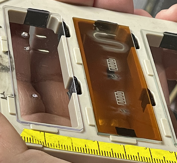
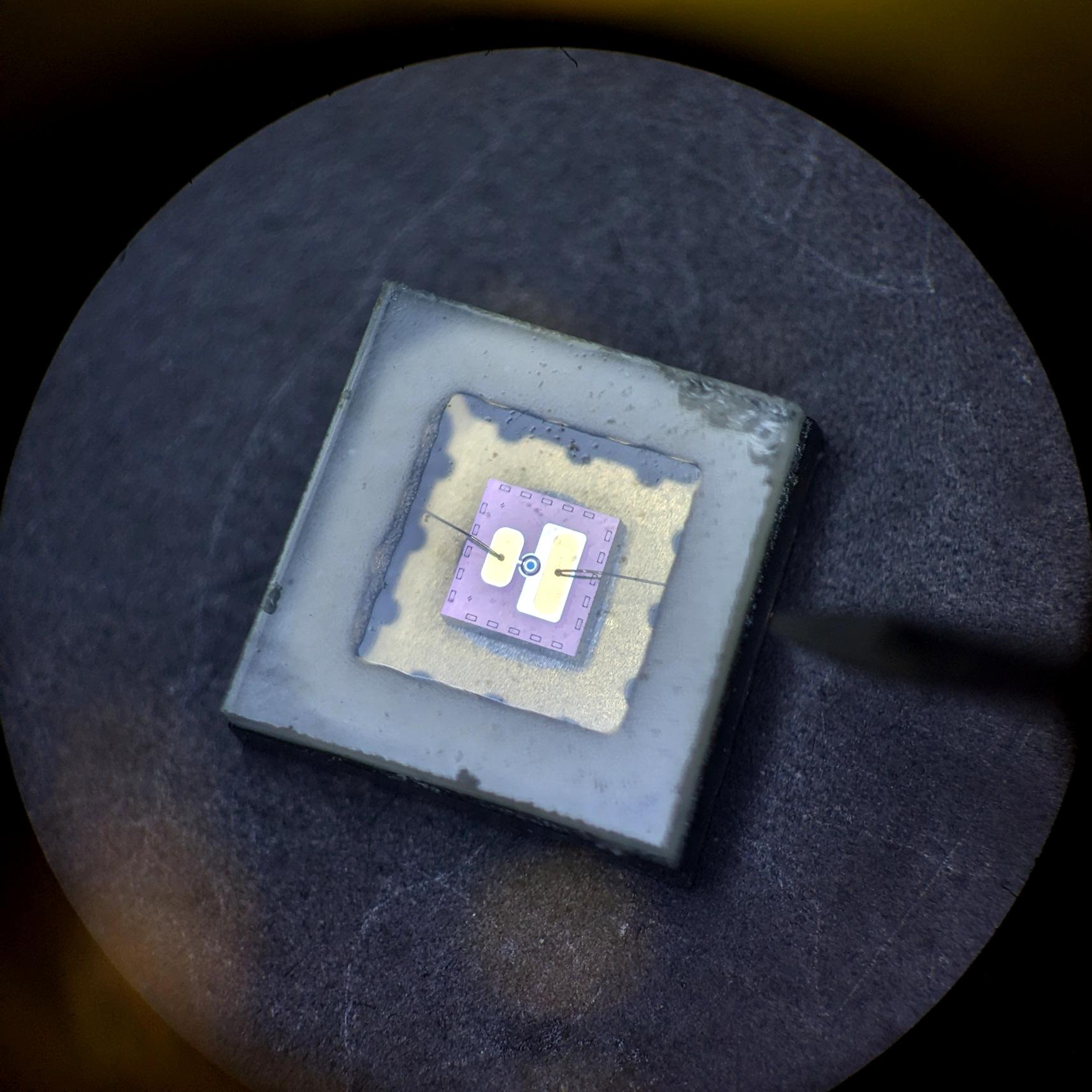
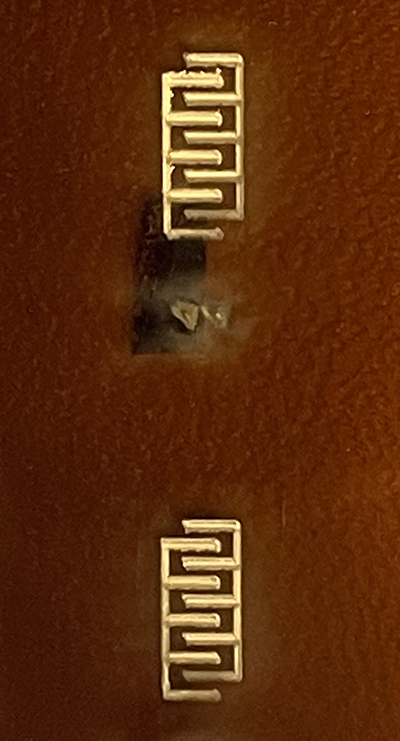
Shown above and below, electrodes that can be used in biological and chemical sensors were printed in the microgravity environment of a zero-G parabolic flight. NASA has been a key supporter of the technology developed by Space Foundry to print electronics with a process involving plasma. Credits: Space Foundry
Space Foundry’s Ram Prasad Gandhiraman, Dennis Nordlund, and senior engineers Pranay Doshi and Daniel Gutierrez testing the company’s plasma 3D printing technology on a NASA-funded parabolic flight. Such flights create microgravity conditions without going to space. Credit: Space Foundry